News
How to reduce the noise of pcb circuit board
How to reduce the noise of pcb circuit board
Many circuit board designers often do perfectly when designing the circuit principle, but every time when debugging, there will always be all kinds of unbearable noises. If you look carefully, you can’t see where the problem is. I can’t find it. Out of the reasons, I had no choice but to redesign a new one. Faced with the problem of noise on the circuit board, Lianxinghua analyzed and summarized the following methods to reduce the noise on the circuit board.
In general, the circuit is partitioned according to the module, and the obvious quiet zone is set between the partitions to minimize the influence of the power supply and the ground on the signal, and to minimize the noise of the circuit board. For specific methods, we will analyze and solve them together.
For a board with good performance, we can see its general distribution at first glance (provided that we know what function of this board is). This is the principle of separation of functional modules that we often say. A functional module is a collection of circuits where some electronic components are combined to complete a certain function. In actual design, we need to bring these electronic components close to reduce the wiring length between the electronic components in order to increase the role of the circuit module. In fact, this is not difficult to understand. Our common development boards or mobile phones do this, especially mobile phones. If you disassemble the mobile phone, you will find that the separation between the various modules is obvious, and each module is Faraday The electric cage is shielded.
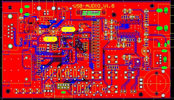
The above picture is a PCB of a development board. From the layout, it can be seen that the separation of each interface circuit is very clear, and the wiring of SDRAM, DDR and SD card interface circuit will not cause mutual interference. By partitioning the system modules, it helps signal integrity, prevents high-frequency interference between system modules, and improves system stability.
Secondly, it should be noted that when there are analog and digital circuits on one, the two need to be separated. If you have to buckle a hat, there will be a quiet zone. The so-called quiet zone is the area that physically separates analog circuits and digital circuits or various functional modules. In this way, you can prevent other modules from interfering with the module. In the mobile phone circuit board mentioned above, the quiet zone is obvious. Note that the quiet zone and the circuit board ground are not connected.
In actual circuit design, not every PCB board has enough space for us to make a quiet zone. Then, when space is not allowed, how should we design? I have summarized the following.
A. Use transformers or signal isolation components for design. We often use CMOS or transistors and other components to form a circuit separation that is the meaning.
B. The signal passes through the filter circuit before entering the module. This method is a common method to prevent ESD. Putting it here is also considering that this method can play a role in eliminating noise (ESD, high-frequency and high-voltage noise).
C. Use common mode inductors for signal protection. This method of circuit protection was once asked by a netizen. If you don't know the role of common mode inductance, we will find in the schematic diagram that there are only two coils, which have no effect. In fact, this is not the case, it plays an important role in the stability of the signal and the elimination of noise interference.
A method similar to the quiet zone is the ditch protection technique. This technique is to remove the divided copper skin in the quiet zone to form a bare circuit board material. The concept of the bridge is also derived from this: the power, ground and signal traces that connect the various sub-zones together are called bridges. The trench protection technology has the ability to withstand the impact of peak voltage and classic discharge protection, which can reduce the noise of the circuit board to a certain extent. In the circuit board design, when the wiring that has nothing to do with the isolation area passes through the protective trench, RF loop current will be generated, which will further affect the performance of the circuit board. This requires attention.
Now, many analog-to-digital or digital-to-analog components have connected the two parts of the ground together inside the component, typically ADC and DAC devices. These devices must have a standard reference ground if the digital signal current Failure to return to the source effectively will cause noise to generate EMI. When drawing the schematic, we found that the pins with AGND and DGND are a device with superior performance, which will reduce the difficulty of our design.
If there is noise on the circuit board, don't rush to redesign one. First try to find out the reason, debug according to the above method, and I will introduce it here, hoping to help everyone.
Latest News
Contact Us
Contact: Ms Tracy
Phone: 0086 18682010757
Tel: 0086 18682010757
Add: Building9,Xinyuan Industrial Park,Tangwei,Fuyong,Baoan,Shenzhen,China
 Tracy
Tracy