26 Layer PCB
26L N4000-13EP+3M C-Ply Buried Capacitor PCB Boards
PCB Detail:
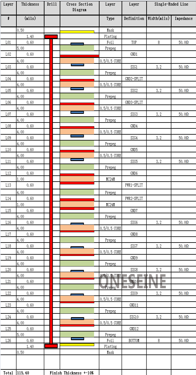
Material:26-Layer PCB Stackup with Nelco 4000-13EP (Ԑr=3.7) for all layers except layers 12-13 and 14-15 which requires MITSUI MC24M material.
Layer:26
Brand:oneseine
Surface finish:ENIG
Stack up
Here are some key points about 26-layer PCBs:
Overview
- A 26-layer PCB is an extremely complex and advanced printed circuit board design, typically used in high-performance, high-density electronics.
- The large number of layers allows for increased component density, more complex routing, and integration of additional power and ground planes.
Applications
- 26-layer PCBs are commonly found in cutting-edge applications like:
- High-speed computing systems (e.g. supercomputers, servers, data centers)
- Advanced military and aerospace electronics
- Complex medical imaging equipment
- Sophisticated telecommunications infrastructure
Manufacturing Challenges
- Fabricating a 26-layer oneseine PCB requires highly specialized equipment, materials, and processes to ensure proper layer registration, trace integrity, and overall board quality.
- Controlling impedances, managing heat dissipation, and minimizing electromagnetic interference (EMI) become increasingly difficult with so many layers.
- The manufacturing process is very complex and expensive compared to lower layer-count PCBs.
Design Considerations
- Extensive use of buried and blind vias is required to interconnect the many layers.
- Careful power plane and ground plane design is crucial to maintain signal integrity.
- Advanced routing algorithms and tools are needed to optimize the complex trace patterns.
- Thermal management through strategic placement of heat-generating components is critical.
Overall, 26-layer oneseinePCBs represent the leading edge of printed circuit board technology, enabling extremely dense and capable electronic systems. However, their complexity demands expert design and manufacturing expertise.
Can you provide an overview of the manufacturing process for 26-layer PCBs?
Certainly, here's an overview of the manufacturing process for 26-layer PCBs:
1. Material Preparation:
- The core materials, typically made of fiberglass-reinforced epoxy resin (FR-4), are precisely cut to size.
- Copper foil is laminated on both sides of the core materials.
2. Inner Layer Processing:
- The inner copper layers are patterned using photolithography and chemical etching to create the desired circuit traces and features.
- Plated through-holes (PTHs) are drilled and plated to provide connections between the layers.
- The inner layers are inspected and cleaned.
3. Lamination:
- The processed inner layers are stacked in the desired order, with prepreg (resin-coated fiber glass) sheets placed between each layer.
- The stack is laminated under high temperature and pressure to bond the layers together.
4. Outer Layer Processing(oneseine):
- The outer copper layers are patterned using photolithography and chemical etching.
- Additional PTHs may be drilled and plated to interconnect the outer layers.
- The outer layers are inspected and cleaned.
5. Final Assembly:
- Components are placed on the outer layers using automated surface mount technology (SMT) equipment.
- The assembled board is subjected to a reflow soldering process to attach the components.
- The board is inspected for any defects or issues.
6. Testing and Quality Control:
- The PCB undergoes a series of electrical and functional tests to ensure it meets the design specifications.
- Rigorous quality control measures, such as visual inspections and X-ray analysis, are performed throughout the manufacturing process.
The manufacturing of 26-layer PCBs requires highly specialized equipment, materials, and expertise to ensure precise layer registration, consistent copper thickness, and reliable interconnections between the numerous layers. The process is generally more complex and time-consuming compared to lower layer-count PCBs, and it often involves close collaboration between the PCB designer and the manufacturer to optimize the design for manufacturability.Oneseine pcb manufacture can do it!
Could you provide more details on the inspection and testing procedures for 26-layer PCBs?
Absolutely, let's dive deeper into the inspection and testing procedures for 26-layer PCBs:
1. Visual Inspection:
- Throughout the manufacturing process, the PCB is visually inspected at various stages to check for defects, such as:
- Misaligned layers
- Missing or damaged plated through-holes (PTHs)
- Copper trace irregularities
- Solder joint quality
- Advanced optical inspection systems are used to capture high-resolution images and identify any anomalies.
2. X-ray Inspection:
- Due to the high layer count, X-ray imaging is essential to inspect the internal layers and interconnections.
- Automated X-ray inspection systems are used to precisely scan the PCB and detect any issues, such as:
- Misaligned or missing PTHs
- Copper trace discontinuities
- Void formations in solder joints
3. Electrical Testing:
- Extensive electrical testing is performed to ensure the correct functionality of the oneseine PCB, including:
- Continuity and resistance measurements
- Insulation resistance testing
- Dielectric withstand voltage testing
- Advanced in-circuit test (ICT) systems are used to automatically test the integrity of the circuit connections and components.
4. Time-Domain Reflectometry (TDR):
- TDR is a crucial technique for 26-layer PCBs to measure and analyze the impedance of the signal traces.
- It helps identify any impedance mismatches, discontinuities, or other issues that could impact signal integrity.
5. Buried Via Inspection:
- With the high density of buried vias in 26-layer PCBs, specialized techniques are employed to inspect their quality, including:
- Scanning acoustic microscopy (SAM) to detect any delamination or voids
- Cross-sectional analysis to visually inspect the internal structure of the vias
6. Environmental Testing:
- 26-layer PCBs may undergo environmental stress testing, such as temperature cycling, humidity, and vibration testing, to ensure reliability under various operating conditions.
The inspection and testing procedures for 26-layer PCBs are more extensive and rigorous compared to lower layer-count boards due to the increased complexity and criticality of the design. These comprehensive quality control measures help ensure the final product meets the stringent performance and reliability requirements of the target application.
What are the key quality control metrics used to assess the reliability of 26-layer PCBs?
When it comes to assessing the reliability of 26-layer PCBs, there are several key quality control metrics that manufacturers closely monitor:
1. Layer Registration and Alignment:
- Ensuring the precise alignment of the 26 individual layers is critical to maintain signal integrity and prevent short circuits.
- Manufacturers measure the registration accuracy between layers to tight tolerances, often within a few microns.
2. Copper Thickness Uniformity:
- Maintaining consistent copper thickness across the various traces, planes, and vias is essential for managing impedances and heat dissipation.
- Variations in copper thickness can lead to signal integrity issues and increased resistance, which can impact the overall performance and reliability.
3. Plated Through-Hole (PTH) Quality:
- With the high density of PTHs in 26-layer oneseine PCBs, the quality and integrity of the plating are crucial.
- Metrics like PTH barrel thickness, wall coverage, and via barrel fill percentage are closely monitored to ensure reliable interconnections between layers.
4. Dielectric Integrity:
- The dielectric materials between the copper layers must maintain their insulating properties to prevent short circuits and signal integrity problems.
- Manufacturers measure the dielectric strength, insulation resistance, and dissipation factor to ensure the dielectric materials meet the design specifications.
5. Impedance Control:
- Maintaining precise control over the characteristic impedance of the signal traces is critical for high-speed digital and RF applications.
- Manufacturers use techniques like time-domain reflectometry (TDR) to measure and validate the impedance of the traces, ensuring they match the desired values.
6. Thermal Management:
- Effective thermal management is crucial for 26-layer PCBs, which can generate significant heat due to the high component density and power dissipation.
- Manufacturers measure the thermal resistance, heat dissipation, and hotspot temperatures to ensure the PCB design can adequately handle the thermal load.
7. Reliability Testing:
- 26-layer PCBs may undergo various reliability tests, such as temperature cycling, humidity exposure, and vibration testing, to assess their ability to withstand environmental stresses.
- Metrics like mean time between failures (MTBF) and failure rates are used to evaluate the long-term reliability of the PCB design.
These quality control metrics are closely monitored and validated throughout the manufacturing process to ensure the 26-layer PCBs meet the stringent reliability and performance requirements of their target applications.
Categories
Latest News
Contact Us
Contact: Ms Tracy
Phone: 0086 18682010757
Tel: 0086 18682010757
Add: Building9,Xinyuan Industrial Park,Tangwei,Fuyong,Baoan,Shenzhen,China
 Tracy
Tracy