High TG PCB
Standard Fr4 TG180 Printed Circuit Boards Multilayer PCB With BGA
- fr4 1.6mm
- high tg 180
- Multilayer pcb
- tg 150-160
- Product description: standard fr4 tg tg 150-160 pcb td pcb gold fingers pcb way login board tg pcb manufacturers pcbway fr4 tg
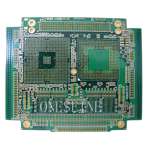
Standard Fr4 TG180 printed circuit boards Multilayer PCB With BGA
Quick detail:
Material:Fr4
Layer:8
Thickness:1.2mm
Surface finish:Immersion gold
Board size:18*22cm
Application:Communication
Name:Multilayer printed circuit boards
Solder mask:Green
Silk screen:White
Multilayer PCB information:
Top silkscreen/Legend: to identify name of each PAD, board part number, data, etc;
Top Surface finishing: to protect exposed copper from oxidation ;
Top Soldermask (overlay): to protect copper from oxidation, to be not soldered during SMT process;
Top Trace: copper etched according to design to carry on different function
Substrate/Core material: Non-conductive such as FR4
Prereg (PP)
Middle Layers, such as GND, VCC, Inner 3, Inner 4, etc.
Prepreg (PP)
Bottom trace (if any): (same as above mentioned)
Bottom soldermask (overlay):(same as above mentioned)
Bottom surface finishing: (same as above mentioned)
Bottom silkscreen/legend: (same as above mentioned)
More layers it is, more complex & difficult the manufacturing will be, and more expensive the cost will be.
Multi-Layer PCB refer to printed circuit board has more than two copper layers, such as 4L, 6L, 8L, 10L, 12L, etc. As technology improving, people can put more and more copper layers on the same board. Currently, we can produce 20L-32L FR4 PCB.
By this structure, engineer can put trace on different layers for different purpose, such as layers for power, for signal transfering, for EMI shielding, for components assembly, and so on. In order to avoid too many layers, Buried Via or Blind via will be designed in multi-layer PCB. For board more than 8 layers, high Tg FR4 material will be popular than normal Tg FR4.
How are multilayer PCBs made?
Alternating layers of prepeg and core materials are laminated together under high temperature and pressure to produce Multilayer PCBs. This process ensures that air isn't trapped between layers, conductors are completely encapsulated by resin, and the adhesive that holds the layers together are properly melted and cured. The range of material combinations is extensive from basic epoxy glass to exotic ceramic or Teflon materials.
The figure above illustrates the stackup of a 4-Layer/ multilayer PCB. Prepeg and core are essentially the same material, but prepeg is not fully cured, making it more malleable than the core.The alternating layers are then placed into a lamination press. Extremely high temperatures and pressures are applied to the stackup, causing the prepeg to "melt" and join the layers together. After cooling off, the end result is a very hard and solid multilayer board.
Categories
Latest News
Contact Us
Contact: Ms Tracy
Phone: 0086 18682010757
Tel: 0086 18682010757
Add: Building9,Xinyuan Industrial Park,Tangwei,Fuyong,Baoan,Shenzhen,China
 Tracy
Tracy