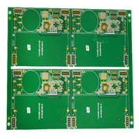
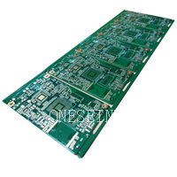
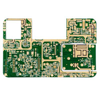
Multilayer PCB
4 Layer Customized Mini Pad Multilayer PCB Maker
- multilayer pcb
- fr4 pcb
- 4 layer pcb
- mini pad pcb
- Product description: 4 Layer Customized Mini Pad Multilayer PCB Maker
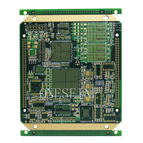
4 Layer Customized Mini Pad Multilayer PCB Maker
Basic technology:
Name:Multilayer printed circuit boards
Layer:4
Material:FR4
Thickness:1.0mm
Copper weight:2OZ
Surface finish:ENIG
Board size:15*8CM
Panel:2*1
Solder mask:Green
Silk screen: White
Multilayer PCB Maker in China:
Do you manufacture advanced electronics and require multilayer circuit boards? Do you need your PCBs in hand as fast as possible? For the best multilayer printed circuit boards and the fastest turn, trust Oneseine Technology. How fast? Same-day turn is available on two-layer PCBs, and 24-hour turn is available on multilayer circuit boards.
Despite our incredibly quick turnaround, we cut zero corners and take zero shortcuts while fabricating multilayer PCBs. In fact, multilayer PCB fabrication requires an even higher level of attention to detail than your average printed circuit board. Care must be taken to ensure all layers are correctly registered despite deformations and stresses produced by the heat and pressure of the multilayer PCB fabrication process. Our highly trained PCB assembly technicians utilize state-of-the-art multilayer circuit board fabrication equipment to ensure that the finished boards we send out meet your exacting standards and technical specifications.
Multi-layer circuit board
Multi-layer circuit board according to the number of wiring surface to determine the process difficulty and processing prices, ordinary sub-single-sided circuit board alignment and double-sided alignment, commonly known as single-sided and double-sided, but high-end electronic products, product space design constraints , In addition to surface wiring, the internal multi-layer lines can be superimposed, the production process, the production of each layer line, and then through the optical device positioning, pressure together, so that multi-layer circuit stack in a circuit board. Commonly known as multi-layer circuit boards. Any greater than or equal to 2 layers of the circuit board, can be called multi-layer circuit board. Multi-layer circuit boards can be divided into multi-layer rigid circuit boards, multi-layer soft and hard circuit boards, multi-layer soft and hard combination of circuit boards.
A multi-substrate is fabricated by stacking two or more circuits with each other, with reliable pre-set interconnections therebetween. Since drilling and electroplating were done before all the layers were rolled together, this technique violated the traditional manufacturing process from the start. The innermost two layers are made of a traditional double-sided board, while the outer layer is different, and they are made of independent single-sided boards. Prior to rolling, the inner substrate will be drilled, plated, patterned, developed, and etched. The outer layer to be drilled is a signal layer which is plated in such a way as to form an equalized copper ring at the inner edge of the through-hole. The respective layers are then rolled together to form a multi-substrate, which can be interconnected using wave soldering (inter-component).
Categories
Latest News
Contact Us
Contact: Ms Tracy
Phone: 0086 18682010757
Tel: 0086 18682010757
Add: Building9,Xinyuan Industrial Park,Tangwei,Fuyong,Baoan,Shenzhen,China
 Tracy
Tracy