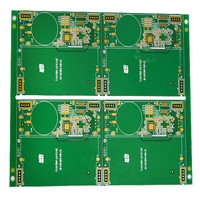
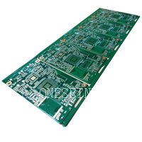
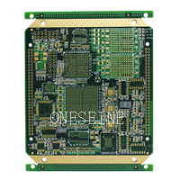
Multilayer PCB
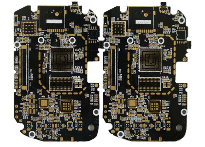
8 Layer Multilayer HDI PCB With Blind Vias Printed Circuit Boards Prototype
- multilayer pcb
- 8 layer pcb
- HDI PCB
- Blind Vias PCB
- Product description: 8 Layer Multilayer HDI PCB With Blind Vias Printed Circuit Boards Prototype
8 Layer Multilayer HDI PCB With Blind Vias printed circuit boards Prototype
General information:
Layer:8
Material:FR4
Thickness: 2.0MM
Surface finish: ENIG
Special: Blind hole,L1-L2,L3-L4,L5-L6,vias filled and capped
Board size:2*6CM
Solder mask:No
Silk screen: White
Name: Multilayer 8Layer Blind Vias PCB Boards
Delivery time: 10days for sample and small&medium batch
About quote:For the special of blind vias pcb,so the accurate quotation have to provide the gerber file(DXP etc.)
Package Details: inner packing:vacuum packing/plastic bag outer packing:standard carton packing
Blind vias:
Blind
vias are used
to connect one outer layer with at least one inner layer.
The holes for each connection level must be defined as a
separate drill file.
The ratio of hole depth to drill diameter (aspect ratio) must be ≤ 1.
The smallest hole determines the depth and thus the max. distance between the
outer layer and the corresponding inner layers.
For detail blind&buried vias pcb
Key words: Microvia, Via-in-Pad
HDI Blind vias PCB:
HDI boards, one of the fastest growing technologies in PCBs, HDI Boards contain blind and/or buried vias and often contain microvias of .006 or less in diameter. They have a higher circuitry density than traditional circuit boards.
There are 6 different types of HDI boards, through vias from surface to surface, with buried vias and through vias, two or more HDI layer with through vias, passive substrate with no electrical connection, coreless construction using layer pairs and alternate constructions of coreless constructions using layer pairs.
Special technologies used with HDI any-layer printed circuit boards:
Edge plating for shielding and ground connection
Minimum track width and spacing in mass production around 40μm
Stacked microvias (plated copper or filled with conductive paste)
Cavities, countersunk holes or depth milling
Solder resist in black, blue, green, etc.
Low-halogen material in standard and high Tg range
Low-DK Material for Mobile Devices
All recognised printed circuit board industry surfaces available
Categories
Latest News
Contact Us
Contact: Ms Tracy
Phone: 0086 18682010757
Tel: 0086 18682010757
Add: Building9,Xinyuan Industrial Park,Tangwei,Fuyong,Baoan,Shenzhen,China
 Tracy
Tracy