Fr4 PCB
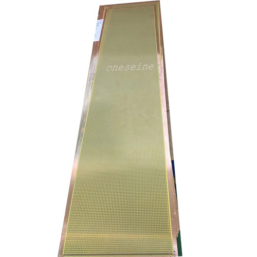
Super Large Super Long FR4 PCB Manufacturer Factory In China
- fr4 pcb
- Super long
- 1 layer pcb
- PCB Circuit Boards
- Product description: custom circuit board assembly small batch pcb manufacturer custom printed circuit board manufacturers fast turnaround pcb pcb fast prototyping small run pcb manufacture pcb manufacturer factory
Super Large Super Long FR4 PCB Manufacturer Circuit Factory In China
PCB Boards specification
Material:Fr4
Boards thickness:1.0
Number of Layer:1
Boards size:1050*350mm
Application: LED
Let me provide some general information about super large PCBs:
Super large PCBs refer to printed circuit boards that are significantly larger in size than typical consumer electronics PCBs. These can range anywhere from 1-2 feet up to several meters in length and width.
Some key characteristics of super large PCBs:
Material: They are most commonly fabricated using FR-4 fiberglass-reinforced epoxy laminate, which provides good structural rigidity at large sizes.
Layer Count: Super large PCBs often have high layer counts, sometimes 8-12 layers or more, to accommodate complex routing and connectivity.
Component Density: Due to the massive size, component placement is more spread out compared to smaller PCBs, with fewer components per square inch.
Manufacturing: Producing these large boards requires specialized equipment and processes, such as large format panel fabrication, automated drilling/routing, and handling systems.
Applications: Super large PCBs are used in industrial machinery, control systems, transportation equipment, renewable energy, and other large-scale applications.
The key design considerations are managing signal integrity, thermal management, mechanical rigidity, and manufacturability across the expansive board real estate.
What are the typical size ranges for super large PCBs?
Small Super Large PCBs:
1-2 feet (30-60 cm) in length and width
Typical for smaller industrial equipment, transportation, or renewable energy applications
Medium Super Large PCBs:
2-4 feet (60-120 cm) in length and width
Commonly used in larger industrial machinery, control panels, and power distribution systems
Large Super Large PCBs:
4-8 feet (120-240 cm) in length and width
Found in very large industrial equipment, transportation vehicles, and renewable energy platforms like wind turbines or solar arrays
Extreme Super Large PCBs:
8 feet (240 cm) and up in both length and width
Reserved for the most massive and complex applications like naval vessels, railway equipment, or utility-scale renewable energy infrastructure
The manufacturing process, material requirements, component placement, and design challenges scale up significantly as the PCB dimensions increase within these size ranges. Specialized equipment, facilities, and engineering expertise are critical for producing and deploying these super large printed circuit boards effectively.
What materials are typically used for the PCB substrate and copper layers in super large boards?
There are some key differences compared to standard sized PCBs:
Substrate Material:
The most common substrate material for super large PCBs is still FR-4 fiberglass-reinforced epoxy laminate.
However, at very large sizes, the panel needs to have exceptional dimensional stability and rigidity. This may require using thicker and/or higher-quality FR-4 material.
Alternative substrates like polyimide or PTFE are sometimes used when even greater dimensional stability is required.
Copper Layers:
Super large PCBs typically have a higher number of copper layers, often 8-12 or more.
The copper foil thickness is also usually thicker, commonly 2-4 oz copper, to provide sufficient current carrying capacity.
Specialized processes are used to laminate and bond the multiple copper layers together without warping or delamination.
Fabrication Processes:
Specialized large-format PCB fabrication equipment is required, including oversized drilling, routing, and plating machines.
Automated handling systems are critical to safely move and process these massive PCB panels.
Enhanced quality control and inspection is needed to ensure uniform performance across the entire board area.
Multi-up panel designs are common to maximize material utilization during fabrication.
Material selection and fabrication techniques are critical for ensuring the final super large PCB has the required structural integrity, electrical performance, and manufacturability. Consulting with experienced PCB fabricators is highly recommended for these types of specialized boards.
Can you provide any examples of applications that require the use of super large PCBs?
Absolutely, there are several key applications that commonly utilize super large PCBs:
Industrial Automation and Machinery:
- Large control panels, motor drives, and other industrial equipment can require PCBs up to 4-8 feet in size.
- These boards integrate power electronics, I/O, and control logic for managing complex industrial processes.
Renewable Energy Systems:
- Solar and wind power generation platforms often use super large PCBs, sometimes over 8 feet, to consolidate power conversion, monitoring, and control functions.
- The large board size allows for efficient routing of high-current electrical connections.
Transportation Vehicles:
- Rail cars, ships, aircraft, and other large vehicles may utilize super large PCBs for central control, power distribution, and sensor integration.
- The large board real estate provides flexibility for component placement and interconnections.
Infrastructure and Utilities:
- Power substations, telecommunications hubs, and other mission-critical infrastructure can require super large PCBs up to several meters in size.
- These boards manage high-power electrical systems, data networks, and monitoring/control functions.
Aerospace and Defense:
- Large avionics and defense electronics systems, such as radar arrays or missile guidance, may leverage super large PCBs.
- The extended board size enables higher component density and simplified wiring/cabling.
The specific size and design requirements vary greatly by application, but the common thread is the need to consolidate complex electrical and electronic functions onto a single, super-sized PCB.
Categories
Latest News
Contact Us
Contact: Ms Tracy
Phone: 0086 18682010757
Tel: 0086 18682010757
Add: Building9,Xinyuan Industrial Park,Tangwei,Fuyong,Baoan,Shenzhen,China
 Tracy
Tracy