PCB Assembly
BGA PCB Printed Circuit Boards Assembly Process Manufacturer in China
- pcba
- pcb assembly
- pcba process
- electronic pcb assembly
- Product description: BGA PCB Printed Circuit Boards Assembly Process Manufacturer in China
BGA PCB printed circuit boards Assembly Process Manufacturer in China
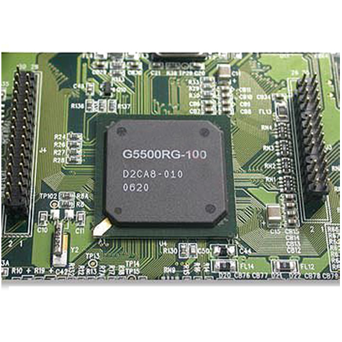
BGA PCB Basic information:
Material:Fr4 1.6mm
Layer:6
Surface finish:Immersion gold
Copper weight:70UM
Assembly components:IC chips(484footprint)
Testing:X-Ray
|
Min line width |
3mil |
|
Min line space |
3mil |
|
Min hole |
0.2mm |
|
Solder mask and silkscreen |
yes |
BGA PCB knowledge:
BGA,means Ball Grid Array, Spherical pin grid array packaging technology, high-density surface mount packaging technology. At the bottom of the package, the pins are spherical and arranged in a lattice-like pattern, so that the name is BGA. At present the motherboard control chipset to use such packaging technology, materials, mostly ceramics. BGA technology with the package of memory, you can make the same size of the memory, the memory capacity increased two to three times, BGA have smaller size thanTSOP , and have better thermal performance and electrical properties. BGA packaging technology greatly improved per square inch of storage , using BGA packaging technology, memory products in the same capacity, the volume is only one-third of TSOP package; compared with the traditional TSOP package, BGA package More efficient and efficient way of cooling.
is a type of surface-mount packaging (a chip carrier) used for integrated circuits. BGA packages are used to permanently mount devices such as microprocessors. A BGA can provide more interconnection pins than can be put on a dual in-line or flat package. The whole bottom surface of the device can be used, instead of just the perimeter. The leads are also on average shorter than with a perimeter-only type, leading to better performance at high speeds.
Soldering of BGA devices requires precise control and is usually done by automated processes. BGA devices are not suitable for socket mounting.
The advantages of BGA pcb
High density
The BGA is a solution to the problem of producing a miniature package for an integrated circuit with many hundreds of pins. Pin grid arrays and dual-in-line surface mount (SOIC) packages were being produced with more and more pins, and with decreasing spacing between the pins, but this was causing difficulties for the soldering process. As package pins got closer together, the danger of accidentally bridging adjacent pins with solder grew. BGAs do not have this problem if the solder is factory-applied to the package.
Heat conduction
A further advantage of BGA packages over packages with discrete leads (i.e. packages with legs) is the lower thermal resistance between the package and the PCB. This allows heat generated by the integrated circuit inside the package to flow more easily to the PCB, preventing the chip from overheating.
Low-inductance leads
The shorter an electrical conductor, the lower its unwanted inductance, a property which causes unwanted distortion of signals in high-speed electronic circuits. BGAs, with their very short distance between the package and the PCB, have low lead inductances, giving them superior electrical performance to pinned devices.
Attention of assembly BGA pcb:
How to plant BGA tin? Some people think that planting tin plate should be up, some people think that should be placed down, otherwise it will be difficult to remove a good chip plant. In fact, how to plant the tin plate is not important, the key is how to plant a good plant after the tin plate and easy separation, and to ensure the success of welding. We all know that the tin paste is composed of tin powder and flux, tin powder melted after the flux out of the cold, then put the cold tin plate and BGA chip firmly stick together. Some people planted tin need to consider the thickness of planted tin plate, they believe that the thickness of the plant after the tin plate will tilt in the heated, steel warp is due to the thermal expansion of the natural law of cold contraction, heating time around the first heating to reduce Temperature, the situation will be greatly improved, do not believe try! Planted tin beads sometimes have the phenomenon of uneven size, just use the scalpel to cut the redundant part of the replantation can be a time. This has a great relationship with the dry and wet tin pulp, tin pulp dry red can add the right amount of welding oil, too thin with the toilet paper to get rid of some "moisture" can be.
Difficulties with BGAs during PCB development
During development it is not practical to solder BGAs into place, and sockets are used instead, but tend to be unreliable. There are two common types of socket: the more reliable type has spring pins that push up under the balls, although it does not allow using BGAs with the balls removed as the spring pins may be too short.
The less reliable type is a ZIF socket, with spring pinchers that grab the balls. This does not work well, especially if the balls are small.
Categories
Latest News
Contact Us
Contact: Ms Tracy
Phone: 0086 18682010757
Tel: 0086 18682010757
Add: Building9,Xinyuan Industrial Park,Tangwei,Fuyong,Baoan,Shenzhen,China
 Tracy
Tracy