Printed Circuit Boards
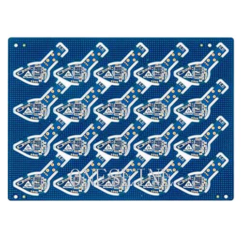
Rogers 4350 0.762mm 4 Layer Blind Hole HDI PCB Board For Bank of the Secret Key
- Buried Blind hole rogers pcb
- rogers pcb board
- Rogers 4350 0.762mm pcb
- 0.762mm
- Product description: What is blind via in PCB? What are vias in double sided PCB? How are buried vias made? What is a plated through hole? pcb blind via fabrication process types of via in pcb pcb antipad plated th
Rogers 4350 0.762mm 4 Layer Blind Hole HDI PCB Board For Bank of the Secret Key
Buried Blind hole rogers pcb board
Rogers high frequency pcb widely used in the area of high technologies like communication device,Electronics,Aerospace,Military industry and so on. we have accumulated abandunt experiences in the line of high frequency microwave business for which widely apply to power divider,combiner,power amplifier,line amplifier,base station,RF antena,4G antena etc.
We have sufficient rogers material raw as follow:RO4003C、RO4350B、RO4360、RO4533、RO4535、RO4730、RO4232、RO4233、RO3003、RO3006、RO3010、RO3035、RO3203、RO3206、RO3210、RO3730、RO5780、RO5880、RO6002、RO3202、RO6006,Frequently-used is 4003C,4350B,5880
So we can do pcb circuit board with your detail requirements in the case of you send us gerber files or any other files
|
Material |
Rogers 4350 |
Layer |
4 |
|
Thickness |
0.8mm |
Board size |
1*1.5cm |
|
Surface finish |
Gold plater |
Panel |
6*8 |
|
Copper |
35UM |
Special |
Blind hole |
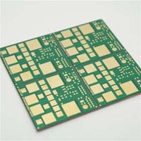
Pcb Board Prototype, Pcb Design And Fabrication
What are PCB through holes, blind holes, buried holes?
Through Hole: Plating Through Hole (PTH), this is the most common type. You just need to pick up the PCB and face the light. You can see that the light hole is the "through hole". This is also the simplest kind of hole, because it is only necessary to use the drill or laser to make the circuit board full drilling, and the cost is relatively cheap. But in contrast, some circuit layers do not need to connect these through holes. For example, we have a six-story house. I bought it on the third and fourth floors. I want to design a staircase inside to connect only the third floor. It can be between the fourth floor. For me, the space on the fourth floor is virtually invisible by the original first floor connecting to the sixth floor stairs. Therefore, although the through hole is cheap, sometimes it will use more PCB space.
Blind hole: Blind Via Hole, which connects the outermost circuit of the PCB to the adjacent inner layer with a plated hole. Because it is not visible, it is called "blind pass". In order to increase the space utilization of the PCB circuit layer, a "blind hole" process has emerged. This method requires special attention to the depth of the hole (Z-axis) to be just right. This method is often difficult to plate in the hole, so it is almost un-manufacturable. It is also possible to connect the circuit layers that need to be connected to the individual circuit layers in advance. At the time, the holes are drilled first and finally glued together, but a more precise positioning and alignment device is required.
Buried hole: Buried hole, the connection of any circuit layer inside the PCB but not to the outer layer. This process can not be achieved by means of bonding after drilling. It is necessary to perform drilling at the time of individual circuit layers. After partially bonding the inner layer, it must be electroplated first, and finally it can be fully bonded, compared with the original "through hole". The "blind hole" takes more time, so the price is also the most expensive. This process is typically only used on high density (HDI) boards to increase the usable space of other circuit layers.
Categories
Latest News
Contact Us
Contact: Ms Tracy
Phone: 0086 18682010757
Tel: 0086 18682010757
Add: Building9,Xinyuan Industrial Park,Tangwei,Fuyong,Baoan,Shenzhen,China
 Tracy
Tracy