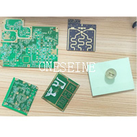
Rogers PCB
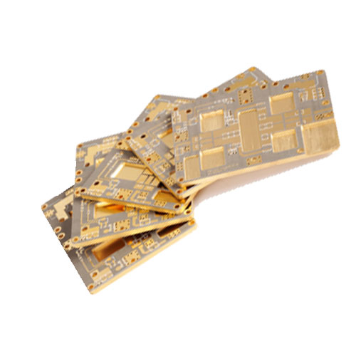
Rogers 3003 0.8mm Thickness Gold Plated High Level Quality PCB Circuit Boards
- rogers pcb
- rogers 3003 pcb
- 0.8mm thickness pcb
- Gold plated pcb
- Product description: Rogers 4003C PCB rogers fr4 pcb stack up pcb Rogers 4360 pcb Rogers Custom PCB Maker Rogers PCB Fabrication rogers pcb price rogers pcb manufacturers rogers pcb prototype rogers pcb calculato
Rogers 3003 Gold Plated High Level Quality PCB Circuit Boards
Quick detail:
Material:High frequency rogers 3003
Layer:2
Surface finish:Gold plated
Board size:6*3cm
Thickness:0.8mm
Copper weight:0.5OZ
Name:rogers 3003 gold plated high level qulity PCB printed circuit boards
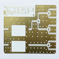
Rogers - High Frequency Circuit Material is glass reinforced hydrocarbon/ceramic laminat ( not PTFE ) designed for performance sensitive, high volume commercial applications
Rogers 3003 PCB:
The RO3003 from Rogers Corp. is a ceramic-filled PTFE composite/laminate for use in commercial microwave and RF applications. It features excellent stability with a dielectric constant of 3 up to 40 GHz at room temperature. The material has a dissipation factor (Df) of 0.0013 at 10 GHz and is ideal for band pass filters, microstrip patch antennas, and voltage controlled oscillators.
By far the most commonly used is the Rogers RO4000 series of high frequency materials.
RO4350B laminate is a hydrocarbon/ceramic base, which can be manufactured using
standard FR-4 type multilayer processes, making it not only popular but economical to
manufacture. Low dielectric loss is the major appealing characteristic of this material.
Multilayers can be constructed of a “pure package” using Rogers 4450 prepreg, or by using standard FR-4 prepreg. Popular constructions limit the Rogers material to the “caps” of the stackup thereby managing overall cost by using the material only where it is required, and filling the remainder of the board with standard FR-4 cores/prepreg.
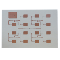
PTFE, commonly known as “Teflon” is another fairly common callout for this genre’s
material requirements. There are many different formulations and laminates such as
Rogers 3000 series ceramic-filled PTFE composites, R/T Duroid 5870 and 5880 glass
microfiber reinforced PTFE, etc. They can be very difficult in multilayer configurations
however, as some require the use of high temperature bonding films or adhesives. The old saying that “nothing likes to stick to Teflon!” sometimes holds true! But their extremely low loss characteristics make them ideal for exacting stripline and microstrip circuit designs.
PCB basic information:
|
Oneseine Technology Go.,LTD |
||
|
Seq |
Item |
capability |
|
1 |
Base Material |
FR-4, High TG FR-4 , Halogen Free material ,CEM-3,CEM-1,PTFE,Rogers ,Arlon ,Taconic,Aluminum base,Teflon,PI ,etc |
|
2 |
Layers |
1-40 ( ≥30 layers needs review ) |
|
3 |
Finished inner/outer copper thickness |
0.5-6OZ |
|
4 |
Finished board thickness |
0.2-7.0mm(≤0.2mm needs review),≤0.4mm for HASL |
|
Board
thickness≤1.0mm: +/-0.1mm |
||
|
5 |
Max panel size |
≤2sidesPCB:
600*1500mm |
|
6 |
Min conductor line width/spacing |
Inner
layers: ≥3/3mil |
|
7 |
Min hole size |
Mechanical
hole: 0.15mm |
|
Drilling
precision: first drilling First drilling:
1mil |
||
|
8 |
Warpage |
Board
thickness≤0.79mm: β≤1.0% |
|
9 |
Controlled Impedance |
+/- 5 % Ω(<50Ω),+/-10%(≥50Ω),≥50Ω+/-5% (needs review) |
|
10 |
Aspect Ratio |
15:01 |
|
11 |
Min welding ring |
4mil |
|
12 |
Min solder mask bridge |
≥0.08mm |
|
13 |
Plugging vias capability |
0.2-0.8mm |
|
14 |
Hole tolerance |
PTH:
+/-3mil |
|
15 |
Outline profile |
Rout/ V-cut/ Bridge/ Stamp hole |
|
16 |
Solder mask color |
Green,yellow,black,blue,red,white,matte green |
|
17 |
Component mark color |
white,yellow,black |
|
18 |
Surface treatment |
OSP:
0.2-0.5um |
|
19 |
E-Test |
Flying probe tester : 0.4-6.0mm,max 19.6*23.5inch |
|
Min spacing from test pad to board edge : 0.5 mm |
||
|
Min conductive resistance : 5 Ω |
||
|
Max insulation resistance : 250 MΩ |
||
|
Max test voltage : 500 V |
||
|
Min test pad diameter : 6 mil |
||
|
Min test pad to pad spacing : 10 mil |
||
|
Max test current : 200 MA |
||
|
20 |
AOI |
Orbotech SK-75 AOI : 0.05-6.0mm,max 23.5*23.5inch |
|
Orbotech Ves machine : 0.05-6.0mm,max 23.5*23.5inch |
||
Categories
Latest News
Contact Us
Contact: Ms Tracy
Phone: 0086 18682010757
Tel: 0086 18682010757
Add: Building9,Xinyuan Industrial Park,Tangwei,Fuyong,Baoan,Shenzhen,China
 Tracy
Tracy