Fr4 PCB
Fr4 Epoxy Resin Laminate Sheet PCB Board
- 8 layer pcb
- 35um outer 17um inner
- hasl lead free
- fr4 pcb
- Product description: fr4 pcb thickness fr4 pcb datasheet fr4 datasheet thickness pcb materials comparison fr-4 specific heat datasheet fr4 epoxy fr4 tg temperature rating of fr4 pcb
Fr4 Epoxy Resin Laminate Sheet PCB Board
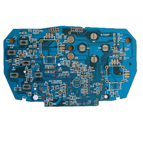
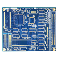
Fr4 PCB Basic Information:
|
Material |
FR4 |
Board size |
8*10cm |
|
Layer |
8 |
Blind hole |
No |
|
Thickness |
1.0mm |
Min line |
3mil |
|
Copper weight |
35um outer 17um inner |
Min hole |
0.3mm |
|
Surface finish |
HASL LF |
Filled plug |
yes |
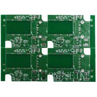
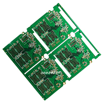
Fr4 PCB boards Manufacturer:
ONESEINE is a professional manufacturer and provide multilayer PCB,high quality ROHS PCB
ONESEINE’s strong fabrication capability and relationship with all material suppliers ensure the production efficiency. We can produce almost full range of PCB products, such as FR4 Board, Aluminum Board, Blind vias Board, HDI Board and so on, widely used in telecommunication, consumer electronics, industrial test and control, medical equipment, power supply, security, network communication, automotive, aviation, research institution and national defense, etc. We has a team of exceptional, proactive and experienced engineering professionals, who strive to ensure the Quality of the custom PCB boards fabrication and assembly services.
HASL Surface finish required to meet ROHS compliant
FR-4 material with 0.4mm-2.6mm board thickness provided
Certificate: ISO UL ROHS REACH
Markets: Europe, North America, South America,Asia etc.
100% TEST (Flying probe testing or E-testing fixture)
With UL,ROHS,ISO,IPC
Lead time:3-10 working days
Competitive price best quality
Rich 9 years experience in Fr4 Multilayer PCB production
Fr4 PCB board layer:
One
layer of copper. Normally the wire-leaded components must be mounted on only
one side of the PCB, with all the leads through holes, soldered and clipped.
You can also mount the components on the track surface using Surface Mount
Technology (SMT) or Surface Mount devices (SMD). Surface mount circuitry is
generally smaller than conventional. Surface mount is generally more suited to
automated assembly than conventional. In practice, most boards are a mix of
surface mount and conventional components. This can have its disadvantages as
the two technologies require different methods of insertion and soldering.
Conventional circuitry is generally easier to debug and repair.
Two layers of copper, one each side of the board. The components must be mounted on only one side of the PCB but you can also mount components on both sides of the PCB. Normally only surface mount circuitry would be mounted on both sides of a PCB. The components must be mounted using both through-holes tecnology or Surface Mount Technology (SMT) or Surface Mount devices (SMD). Conventional circuitry is generally easier to debug and repair.
A PCB Laminate may be manufactured with more than two layers of copper tracks by using a sandwich construction. The cost of the laminate reflects the number of layers. The extra layers may be used to route more complicated circuitry, and/or distribute the power supply more effectively.
Fr4 PCB board layout:
The PCB layout can be draw either manually or by ECAD (Electronic - Computer Aid Design) software. The manual process is useful and quick only for very easy PCBs, for more complex PCBs I suggest the second way. Nowadays inexpensive computer software can handle all aspect of PCBs pre-processing. Also is available expensive professional computer software that can direct control the fabrication processing tools
Categories
Latest News
Contact Us
Contact: Ms Tracy
Phone: 0086 18682010757
Tel: 0086 18682010757
Add: Building9,Xinyuan Industrial Park,Tangwei,Fuyong,Baoan,Shenzhen,China
 Tracy
Tracy