Printed Circuit Boards
6 Layer 10 OZ Heavy Copper PCB Printed Circuit Boards
- 10 OZ
- heavy copper
- Board Thickness: 2.0mm
- Surface Process: ENIG
- Product description: metal core pcb pcb copper thickness pcb copper thickness chart pcb copper thickness calculator pcb trace pcb manufacturing 7 oz copper pcb pcb assembly china
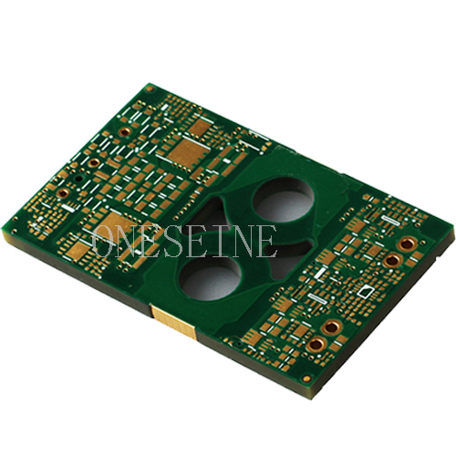
6 Layer 10 OZ Heavy Copper PCB printed circuit boards
Board information:
Layer: 6 Layer PCB
Name: heavy copper PCB
Material: FR4 PCB
Board size: 11*17cm
Surface finish: HASL lead free
Copper weight:10 OZ
Board thickness:2.0MM
Special: L1-L2,L3-L4,L5-L6 blind hole
Solder mask: Green
Silkscreen: white
Delivery time: 12 working days
Heavy copper PCB define:
Heavy copper pcb also can be called thick copper pcb or copper pcb
In the PCB field, haven’t exact define to the thick copper pcb,but generally,more than 2OZ pcb we call it thick copper pcb.Heavy copper pcb mainly used in the products with Voltage and current are relatively high
For more detail heavy copper pcb information,please click here
Some special methods of manufacturing printed circuit board with thick copper PCB:
The heavy copper features can be seamlessly connected to standard circuits. Heavy copper and standard features can be placed with minimal restriction provided the designer and fabricator discuss manufacturing tolerances and abilities prior to final design
Standard printed circuit boards, whether double-sided or multilayer, are manufactured using a combination of copper etching and plating processes. Circuit layers start as thin sheets of copper foil (generally 0.5 oz/ft2 to 2 oz/ft2) that are etched to remove unwanted copper, and plated to add copper thickness to planes, traces, pads and plated-through-holes. All of the circuit layers are laminated into a complete package using an epoxy-based substrate, such as FR4 or polyimide.
Boards incorporating heavy copper circuits are produced in exactly the same way, albeit with specialized etching and plating techniques, such as high-speed/step plating and differential etching. Historically, heavy copper features were formed entirely by etching thick copper clad laminated board material, causing uneven trace sidewalls and unacceptable undercutting. Advances in plating technology have allowed heavy copper features to be formed with a combination of plating and etching, resulting in straight sidewalls and negligible undercut.
Plating of a heavy copper circuit enables the board fabricator to increase the amount of copper thickness in plated holes and via sidewalls. It's now possible to mix heavy copper with standard features on a single board. Advantages include reduced layer count, low impedance power distribution, smaller footprints and potential cost savings. Normally, high-current/high-power circuits and their control circuits were produced separately on separate boards. Heavy copper plating makes it possible to integrate high-current circuits and control circuits to realize a highly dense yet simple board structure.
The benefits of heavy copper in PCBs:
Reduction of thermal strain
Better current conductivity
Can survive repeated thermal cycling
Smaller PCB size due to layering of copper
Increased connector site strength
Categories
Latest News
Contact Us
Contact: Ms Tracy
Phone: 0086 18682010757
Tel: 0086 18682010757
Add: Building9,Xinyuan Industrial Park,Tangwei,Fuyong,Baoan,Shenzhen,China
 Tracy
Tracy