Fr4 PCB
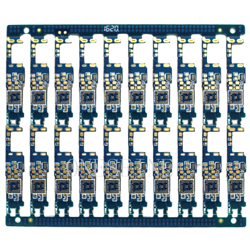
Bluetooth Module Fr4 4 Layer Gold Plated Side PCB Boards Prototype
- bluetooth module pcb
- 4 layer pcb
- gold plated pcb
- 1.2mm thickness
- Product description: pcb gold plating thickness enig pcb pcb shelf life pcb plating disadvantages of pcb osp pcb immersion tin plating enig process steps
Bluetooth Module Fr4 4 Layer Gold Plated Side PCB Boards Prototype
PCB information:
|
Layer |
4 |
Copper |
1OZ |
|
Material |
Fr4 |
Size |
3*1.5cm |
|
Thickness |
1.2mm |
Color |
Blue |
|
Surface |
Gold plated |
Min line |
4mil |
Gold Plated PCB Purpose:
For the noise generated by the vias, we know that the signal lines interconnected on the PCB include the microstrip line of the outer layer of the pcb, the strip line with the inner layer lying between the two planes, and the plated vias whose signals are exchanged for layer connection (via holes are fine). Divided into through holes, blind holes, buried holes), the microstrip line in the surface layer and the strip line in the two planes can be well controlled by a good reference plane layered structure design.
The vias penetrate multiple layers in the vertical direction. When high-frequency signal transmission lines are layered through vias, not only the impedance of the transmission line changes, but also the reference plane of the signal return path changes, when the frequency of the signal is relatively low. When it is low, the effect of vias on signal transmission is negligible. However, when the signal frequency rises to the RF or microwave frequency range, the TEM waveform generated by the via will change due to the change of the current return path caused by the reference plane change of the via. In the two planes formed between the resonant cavity of the lateral propagation, and ultimately radiated to the free space through the pcb's edge, causing EMI indicators exceeded.
Now we know that for high-frequency high-speed PCBs, there will be edge radiation problems on the edge of the PCB. How do we protect it?
The three elements that create EMC problems are: electromagnetic interference sources, coupling paths, and sensitive equipment
Sensitive equipment we can not control, cut off the coupling path, such as adding a metal shielding device shell, the old wu do not speak here, how to find ways to get rid of the interference source.
First, we must optimize the critical signal traces on the PCB to avoid EMI problems. We must use ground vias on the vias of key signals to provide additional return paths for key signal vias. .
In order to reduce the effect of edge radiation, the power plane should shrink in comparison with the adjacent ground plane, and the effect is not obvious when the power plane shrinks by about 10H. When the power plane shrinks by 20H, it absorbs 70% of the Flux Boundary. When the power plane shrinks 100H, it can absorb 98% of the marginal flux boundary; thus shrinking the power layer can effectively inhibit the radiation caused by the marginal effect.
For the microwave circuit board, the wavelength is further reduced, and due to the PCB manufacturing process, the gap between the hole and the hole can not be made very small. At this time, the 1/20 wavelength interval has been used to shield the PCB around the via hole. The role of the microwave board is not so obvious. At this time, the PCB version metalized edging process is needed to surround the entire board with metal so that the microwave signal cannot be radiated from the PCB board edge. Of course, the board edge metallization is used. The edging process will also lead to a significant increase in the manufacturing cost of the PCB.
Categories
Latest News
Contact Us
Contact: Ms Tracy
Phone: 0086 18682010757
Tel: 0086 18682010757
Add: Building9,Xinyuan Industrial Park,Tangwei,Fuyong,Baoan,Shenzhen,China
 Tracy
Tracy