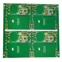
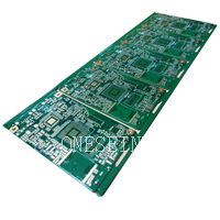
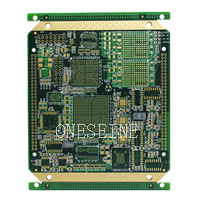
Multilayer PCB
6 Layer Custom Multilayer PCB Fabrication
- 6 layers pcb
- custom pcb
- Multilayer pcb
- pcb fabrication
- Product description: multilayer pcb manufacturing process steps multilayer pcb design diy multilayer pcb how to identify a multilayer pcb printed circuit board manufacturing process multilayer pcb printer multilayer
6 Layer Custom Multilayer PCB Fabrication
Basic information:
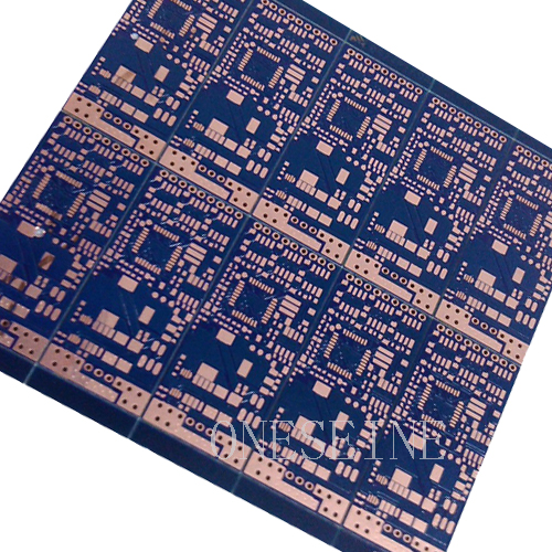
Size:11*7CM
Layer:6
Surface finish: Immersion gold
Thickness:1.6mm
Copper weight:1.5OZ outer
Color:Blue solder mask
PCB Classify:
Rigid
PCB
Single-sided, double-sided & multi-layer PCB (up to 30 layers) HDI,High TG
Multilayer,Heavy
Copper,Gold
Finger,Blind Buried Holes PCB,Impedance PCB and other special process.
Flexible & Rigid-flex PCB
Flexible PCB (up to 10 layers) & Rigid-flex PCB (up to 8 layers)
Metal Core PCB
Single/Double-Sided Aluminium Base PCB and Copper Base PCB
PCB Material
CEM-1,CEM-3,FR-4,High TG,Polyimide, Aluminum and Copper-based material.
PCB Surface Technics
HAL, HAL lead free, Immersion Gold/ Silver/Tin, Hard Gold, OSP
Multilayer PCB Introduction:
The manufacturing method of the multilayer PCB board is generally performed by the inner layer pattern first, and then the single-sided or double-sided substrate is formed by the printing etching method, and is incorporated into the specified interlayer, and then heated, pressurized and bonded, and the subsequent drilling is performed. Holes are the same as double-sided plated through holes
Plated through hole
Once copper
After the formation of the via hole in the interlayer, it is necessary to build a copper layer on it to complete the conduction of the interlayer circuit. Firstly, brushing and high-pressure flushing are used to clean the dust on the holes and pores, and then remove the smear on the copper surface of the pore wall with potassium permanganate solution. A tin-palladium colloid layer is immersed in the cleaned pore wall and then reduced to metallic palladium. The circuit board is immersed in a chemical copper solution, and palladium ions in the solution are used to reduce the copper ions in the solution and deposit on the wall of the hole to form a via circuit. Then, the copper layer in the via hole is thickened by a copper sulfate bath to sufficiently resist the thickness of the subsequent processing and use of the environmental impact.
Outer line
Secondary copper
In the production of circuit image transfer printing, it is similar to the inner layer circuit, but in the line etching, it is divided into two kinds of production methods: positive and negative. The production method of the negative film is the same as that of the inner layer circuit. After the development, the copper is directly etched and the film is removed. The production method of the positive film is to apply the secondary copper and tin-lead plating after the development (the tin-lead in this area will be retained as an etching resist in the later copper etching step), and the film will be alkaline after the film is removed. Aqueous ammonia and copper chloride mixed solution etch away the exposed copper foil to form a circuit. Finally, tin and lead stripping solution was used to strip the tin and lead layers that had been retired. (In the early days, there were tin and lead layers that had been reserved, and after being used as a cover layer, they were used as a house-keeping layer. Now, they are not needed.) .
Anti-welding edge paint
After the outer layer circuit is completed, it needs to be covered with an insulating resin layer to protect the household circuit from oxidation and welding short circuit. Before the coating, the copper surface of the circuit board must be properly roughened and cleansed by brushing and micro-etching. Afterwards, the liquid photosensitive green paint is applied to the board surface by means of steel plate printing, curtain coating, electrostatic spraying, etc., and then pre-baked and dried (dry film photosensitive green paint is laminated by a vacuum laminator. On the board). When it is cooled, it is sent to an ultraviolet exposure machine for exposure. The green paint will produce a polymerization reaction after being exposed to ultraviolet rays in the light-transmitting area of the film (the green paint in this area will be retained in a later development step), with a solution of sodium carbonate. Undeveloped areas of the film were developed and removed. Finally, high-temperature baking was performed to completely harden the resin in the green paint.
Categories
Latest News
Contact Us
Contact: Ms Tracy
Phone: 0086 18682010757
Tel: 0086 18682010757
Add: Building9,Xinyuan Industrial Park,Tangwei,Fuyong,Baoan,Shenzhen,China
 Tracy
Tracy