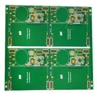
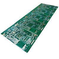
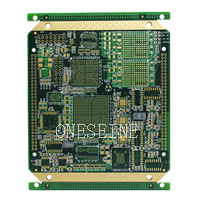
Multilayer PCB
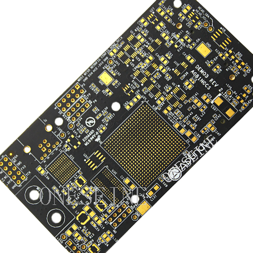
14 Layer PCB HDI Vias in Pad BGA Printed Circuit Board
- 14 layer
- vias in pad
- HDI
- stack up PCB
- Product description: 14 Layer PCB HDI Vias in Pad BGA Printed Circuit Board
14 Layer PCB HDI Vias in Pad BGA printed circuit board
PCB introduction:
|
Layer |
14 |
Color |
Black |
|
Material |
Fr4 |
Min hole |
0.15 |
|
Surface |
Gold plated |
Special |
Vias in pad |
|
Min line |
4mil |
BGA |
2 |
14 Layer Fr4 Via-In-Pad PCB printed circuit board
Perhaps one of the greatest benefits of via fill is the option to implement Via In-Pad. This process is becoming more and more popular and preferred as opposed to using the traditional "dog bone" method to transfer signal from the BGA, through the via, and on to inner layers. In this process, also known as active pad, vias are filled, planarized, plated over with copper. While the Via-In-Pad process does increase cost there can be significant benefits over conventional through hole technology.
Some key benefits are:
Tighter BGA pitches
Increased thermal dissipation
Reduced layer count or board size, which ultimately may reduce cost
Improved routing density (higher density per layer)
Strengthening Pad attachment
Gives high frequency designs the shortest possible route to bypass capacitors
Overcomes high speed desogn issues and constraints such as low inductance
Via in pad technology gets you intermediate density at a slightly higher cost compared to blind/buried vias. The extra dollars go into added manufacturing steps and material cost. But the benefits you get are:
Fan out fine pitch (less than .75mm)
Meets closely packed placement requirements
Better thermal management
Overcomes high speed design issues and constraints i.e. low inductance
No via plugging is required at component locations
Provides a flat, co-planar surface for component attachment
What is prepreg in PCB?
Prepreg, which is an abbreviation for pre impregnated, is a fibre weave impregnated with a resin bonding agent. It is used to stick the core layers together. The core layers being FR4 with copper traces. The layer stack is pressed together at temperature to the required board finish thickness.
14 Layer pcb stack up
What is layer stackup?
The PCB stackup is the substrate upon which all design components are assembled. A poorly designed PCB stackup with inappropriately selected materials can degrade the electrical performance of signal transmission, power delivery, manufacturability, and long term reliability of the finished product.
How many layers can a PCB have?
It is usually even and includes the two outer layers. Most main boards have between 4 and 8 layers, but PCBs with almost 100 layers can be made
14 layer and 16 Layer also common orders here in Oneseine
Categories
Latest News
Contact Us
Contact: Ms Tracy
Phone: 0086 18682010757
Tel: 0086 18682010757
Add: Building9,Xinyuan Industrial Park,Tangwei,Fuyong,Baoan,Shenzhen,China
 Tracy
Tracy