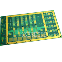
High Frequency PCB
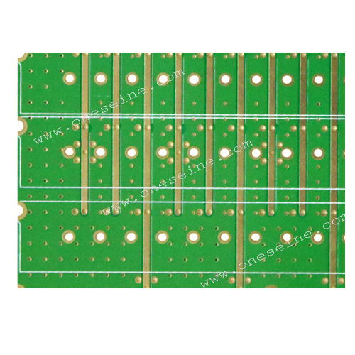
Rogers 3003 material Circuit board manufacture of pcb
- HF PCB
- 2 Layer pcb
- rogers 3003
- Immersion gold(ENIG)
- Product description: manufacture of pcb printed circuit manufacturing circuit boards manufacturing pcb manufacturing manufacturing pcb boards
Rogers 3003 material Circuit board manufacture of pcb
Material:rogers3003 0.635MM
DK:3
Layer:2
Surface finish: immersion gold
Application:Microwave / RF field
Board thickness:0.8MM
Min lind width and space:8mil
Min hole:0.3MM
Importance to Understanding of manufacture of pcb
When reply to the question “Is it important to understand the PCB fabrication process?”, purchasers may have no interest because they are only responsible for PCB procurement -release orders to the PCB manufacturer, supplier or provider, and receive the PCB boards at the due date. While, electrical and electronic designers may have interest. PCB manufacturing is not a design activity, but when a designer understands the circuit board fabrication process, his design would be more mature and manufacturable with low cost and high quality.
PCB manufacturing process is performed by a printed circuit boards (PCB) manufacturer, all manufacturing activities will accord to the specifications that provided by the outsourcing company, and as per IPC related standards. In most cases, manufacturers are not privy to your PCB design intent or performance objectives, but they will conduct DRC, DFM and DFA checks for you. Therefore, they would not be aware of whether you are making good choices for materials, stack-up, routing, via locations and types, trace widths/spacings or other PCB parameters that design during PCB board fabrication and may impact your PCB’s manufacturability, production yield rate or performance after deployment, as listed below:
Manufacturability: Whether your PCB is manufacturable depending on a number of design choices, which are including but not limited to keeping adequate spaces between trace and trace, between trace and pad, between pad and pad, between trace and PCB edge, between pad and legend, between trace and drills and etc. as well as annular ring, via structure, via protection type, surface finish, stack-up (thru-hole, buried or blind), slot minimum width, half-hole minimum drilling diameter, material choice (Tg, Dk, Df, CTE, PP, adhesive or adhesiveless PI base for FPC), profile shape, and others. Either of these could result in the inability of your PCB board being fabricated without redesign or re-layout. What’s more, if your PCB is tiny and you decide to panelize it, then you need to confirm with your PCB fabricator whether it’s manufacturable and with maximum material usage rate.
Production Yield: When your design passes the process of CAM engineering, your PCB seems will be successfully fabricated if following the manufacturing instructions (MI) and other documentations, while fabrication issues may still exist or be in risk of quality. This will reduce the production yield, i.e. quality passing rate. For instance, your fabrication drawings specify tight tolerances that beyond the limits of your PCB manufacturer’s equipment, that will result in higher than acceptable of boards that are unusable.
Categories
Latest News
Contact Us
Contact: Ms Tracy
Phone: 0086 18682010757
Tel: 0086 18682010757
Add: Building9,Xinyuan Industrial Park,Tangwei,Fuyong,Baoan,Shenzhen,China
 Tracy
Tracy