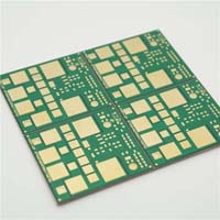
Printed Circuit Boards
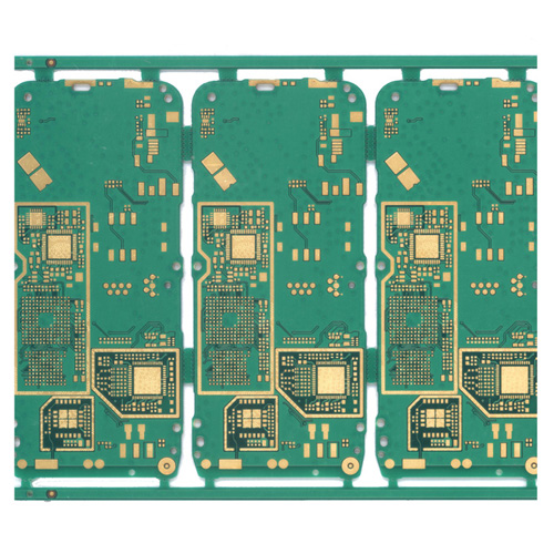
Fr4 Multilayer Controlled Impedance PCB Trace 50ohm±5%
- Controlled Impedance PCB
- Trace 50ohm±5%
- Multilayer pcb
- fr4 pcb
- Product description: when to use controlled impedance 50 ohm controlled impedance what is impedance matching in pcb how to specify pcb impedance an introduction to the design and manufacture of controlled impedance pc
Fr4 Multilayer Controlled Impedance PCB Trace 50ohm±5%
Quick detail:
|
PCB layer |
Materials |
|
· Multilayer PCB with 8 layers |
· Fr4 |
|
PCB thickness |
Final copper |
|
· 2.6 mm |
· 2OZ |
|
Conductor track widths |
Minimum drilling diameter |
|
· ≥ 90 µm |
· 0.2 mm |
|
Contour production |
Solder masks |
|
· Milling · Scoring |
· Photosensitive solder mask systems · UV solder mask system, screen printing |
|
Surfaces |
Additional printing |
|
Immersion gold |
· Impedance 50ohm PCB |
Manufacture of Controlled Impedance PCBs,Impedance PCB prototype, Controlled impedance PCB fabrication
50 ohm controlled impedance PCB, pcb trace resistance calculator, pcb trace impedance
Parameter:
|
Layer |
12-26 |
|
Material type |
FR-4, CEM-1, CEM-3, High TG, FR4 Halogen Free, Rogers |
|
Board thickness |
0.21mm to 7.0mm |
|
Copper thickness |
0.5 OZ to 6 oz |
|
Size |
Max. Board Size: 580mm×1100mm |
|
Min. Drilled Hole Size: 0.2 mm (8 mil) |
|
|
Min. Line Width: 4mil (0.1mm) |
|
|
Min. Line Spacing: 4mil (0.1mm) |
|
|
Surface finishing |
HASL / HASL lead free, HAL, Chemical tin, |
|
Solder Mask Color |
Green/Yellow/Black/White/Red/Blue |
|
Tolerance |
Shape tolerance: ±0.13 |
|
Hole tolerance: PTH: ±0.076 NPTH: ±0.05 |
|
|
Certificate |
UL, ISO 9001, ISO 14001 |
|
Special requirements |
Buried and blind vias+controlled impedance +BGA |
|
Profiling |
Punching, Routing, V-CUT, Beveling |
Impedance pcb definition:
· Impedance board is defined as: a good laminated structure can play on the printed circuit board characteristic impedance control, the alignment can be easily controlled and predictable transmission line structure called the impedance pcb
· Impedance is the sum of the resistance and reactance of an electrical circuit expressed in Ohms. The resistance being the opposition to current flow present in all materials. The reactance is the opposition to current flow resulting from the effect of the inherent capacitance and inductance of the conductor interacting with changes in voltage and current. In DC circuits there is no reactance and the resistance of copper conductors is typically insignificant. However in high speed AC circuits (those with sharp changes in voltage and/or current) the reactance and thus the impedance can become very significant. This can become critical to a design's functionality because of the effects that changes in the impedance along the signals path from transmitter to receiver will have on the efficiency of power transfer as well as signal integrity. While a circuit’s speed is often expressed as the frequency of the wave form: the critical concern is the speed at which the voltage and/or current is required to change..
· One of the most common examples of controlled impedance is the cable that connects the antenna to your television. That cable may be a coaxial cable consisting of a round, inner conductor, separated from the outer cylindrical conductor commonly called the shield by an insulator. The dimensions of the conductors and insulator, and the electrical characteristics of the insulator are carefully controlled in order to determine the shape, strength and interaction of their electrical fields which will determine the electrical impedance of the cable.
Similarly there are many different trace configurations that are used in printed circuit boards to achieve controlled impedance.
· Controlled impedance boards use a plane layer as the shield, the laminate as the insulator and the conductor is the trace. The impedance of the trace on the board is determined by its dimensions, the materials used.
· Impedance is measured in Ohms but is not to be confused with resistance. Resistance is a direct current characteristic; impedance is an alternating current characteristic that includes signal frequency. Signal frequency is critical for those traces connecting to components requiring two or three hundred MHz and above.
What is Controlled Impedance?
· Unless you have carefully designed the trace and its environment, impedance is typically "uncontrolled", meaning that impedance will vary in value from point to point along the trace.
· At high frequencies, PCB traces do not behave like simple connections, controlled impedance helps us ensure that signals are not degraded as they route around a PCB.
· Essentially, controlled impedance is the matching of substrate material properties with trace dimensions and locations to ensure the impedance of a trace's signal is within a certain percentage of a specific value. Controlled impedance boards provide repeatable high frequency performance.
· When a signal must have a particular impedance in order to function properly, controlled impedance should be used. In high frequency applications matching the impedance of PCB traces is important in maintaining data integrity and signal clarity. If the impedance of the PCB trace connecting two components does not match the components' characteristic impedance, there may be increased switching times within the device or the circuit. There may also be random errors.
· The characteristic impedance of a PCB trace is typically determined by its inductive and capacitive reactance, resistance, and conductance. These factors are a function of the physical dimensions of the trace, the dielectric constant of the PCB substrate material, and dielectric thickness. Typically PCB trace impedance can range from 25 to 125 ohms
Impedance calculate:
The rising edge time of the signal and the proportional relationship of the time required for signal transmission to the receiver determine whether the signal connection is considered to be a transmission line. Specific proportional relationship can be explained by the following formula: If the PCB board wire length is greater than l / b can be the signal between the connecting wire as a transmission line. From the signal equivalent impedance formula we can see that the transmission line impedance can be expressed by the following formula: in the high frequency (tens of megahertz to several hundred MHz) to meet wL >> R Taking into account the signal skin effect, need to carefully study this relationship). Then the characteristic impedance for a given transmission line is a constant. Signal reflection phenomenon is due to the signal drive side and the transmission line characteristic impedance and the impedance of the receiver side caused by inconsistency. For the CMOS circuit, the signal output impedance of the drive side is relatively small, for the dozens of Europe. While the receiving end of the input impedance is relatively large.
Categories
Latest News
Contact Us
Contact: Ms Tracy
Phone: 0086 18682010757
Tel: 0086 18682010757
Add: Building9,Xinyuan Industrial Park,Tangwei,Fuyong,Baoan,Shenzhen,China
 Tracy
Tracy