Printed Circuit Boards
One Stop PCB Layout Printed Circuit Board Design
- one stop
- pcb design
- pcb layout
- fr4 pcb
- Product description: pcb layout tutorial how to make pcb layout pcb layout software pcb layout diagram pcb layout online pcb layout design pdf how to make pcb layout from circuit diagram pcb layout service
One Stop PCB Layout Design
Although the printed circuit board engineers are not involved in the design of PCBs, by the customer out of the original design information and then made the company's internal PCB circuit board production information, but through years of practical experience, engineers have accumulated on the PCB circuit board design, summarized as follows for reference only:
Printed circuit board design process including schematic design, electronic components database login, design preparation, block division, electronic components, configuration confirmation, wiring and final inspection. In the course of the process, no matter which process found a problem, must return to the previous operation, re-confirmed or amended.
PCB design steps:
1,According to the circuit function needs to design schematic diagram. Schematic design is based on the electrical properties of components according to the need for reasonable structures, through the diagram can accurately reflect the important functions of the PCB circuit board, and the relationship between the various components. Schematic design is the first step of PCB production process, is also very important step. Usually the software used to design the circuit schematic is PROTEl.
2, After finish the schematic design, you need a closer step by PROTEL on the various components of the package, to generate and implement components with the same appearance and size of the grid. After editing the component package, execute Edit / Set Preference / pin 1 to set the package reference point to the first pin, and then execute the Report / Component Rule check to set the rules to be checked.
3, Formal PCB generation. After the network is generated, it is necessary to position each component according to the size of the PCB panel, and to ensure that the leads of the individual components do not intersect when placed. Place components after the completion of the final DRC check to rule out the wiring of the various components of the pin or lead cross error, when all the errors are excluded, a complete pcb design process is complete.
4, The PCB was designed printout through the inkjet printer, and then put the side with printed circuit diagram impact copper board, and finally into the heat exchanger for hot printing, through the high temperature will copy paper Circuit diagram The ink sticks to the copper plate.
5, Make board. The solution was prepared by mixing sulfuric acid and hydrogen peroxide at a ratio of 3: 1 and then placing the copper plate containing the ink therein for about three to four minutes. After the copper plate was completely etched away from the ink, , Then rinse the solution out with clear water.
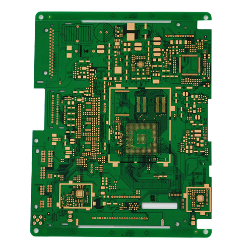
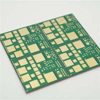
Our PCB layout and PCB design services and capabilities include:
Single-sided, double-sided, and multi-layer boards
Rigid and flexible circuits
Surface mount, through-hole, mixed technology
Design for manufacturability (DFM)
Design for testability (DFT)
Design for EMC
PCB design:
Initially PCBs were designed manually by creating a photomask on a clear mylar sheet, usually at two or four times the true size. Starting from the schematic diagram the component pin pads were laid out on the mylar and then traces were routed to connect the pads. Rub-on dry transfers of common component footprints increased efficiency. Traces were made with self-adhesive tape. Pre-printed non-reproducing grids on the mylar assisted in layout. To fabricate the board, the finished photomask was photolithographically reproduced onto a photoresist coating on the blank copper-clad boards.
Modern PCBs are designed with dedicated layout software, generally in the following steps:
Schematic capture through an electronic design automation (EDA) tool.
Card dimensions and template are decided based on required circuitry and case of the PCB.
The positions of the components and heat sinks are determined.
Layer stack of the PCB is decided, with one to tens of layers depending on complexity. Ground and power planes are decided. A power plane is the counterpart to a ground plane and behaves as an AC signal ground while providing DC power to the circuits mounted on the PCB. Signal interconnections are traced on signal planes. Signal planes can be on the outer as well as inner layers. For optimal EMI performance high frequency signals are routed in internal layers between power or ground planes.[5]
Line impedance is determined using dielectric layer thickness, routing copper thickness and trace-width. Trace separation is also taken into account in case of differential signals. Microstrip, stripline or dual stripline can be used to route signals.
Components are placed. Thermal considerations and geometry are taken into account. Vias and lands are marked.
Signal traces are routed. Electronic design automation tools usually create clearances and connections in power and ground planes automatically.
Gerber files are generated for manufacturing.
Categories
Latest News
Contact Us
Contact: Ms Tracy
Phone: 0086 18682010757
Tel: 0086 18682010757
Add: Building9,Xinyuan Industrial Park,Tangwei,Fuyong,Baoan,Shenzhen,China
 Tracy
Tracy