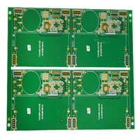
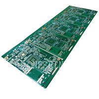
Multilayer PCB
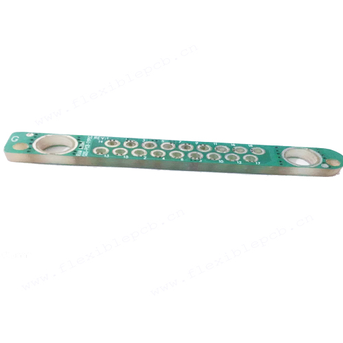
Super thick Integrated Circuit Board pcb fabrication services
- Mix stack up pcb
- super thick
- pcb fabrication
- Immersion gold(ENIG)
- Product description: Integrated Circuit Board pcb fabrication companies quick turn pcb fabrication circuit board fabrication fabrication board pcb fabrication services pcb fab house board fabrication low cost pcb
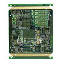
FR4 Super thick Integrated Circuit Board pcb fabrication services
Material:FR4
Layer:8
Surface finish:ENIG
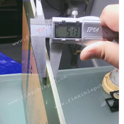
Thickness:5mm
What Information customer need to provide for quotation ?
1. PCB Gerber files ,protel,powerpcb,Autocad,etc.
2. BOM list for PCB assembly.
3. Send us your sample PCB or PCBA.
Competitive Advantage:
1) With UL,ROHS,ISO,IPC
2).Lead time:3-10 working days
3)Competitive price best quality
4).Rich 20 years experience in High Tg Multilayer PCB .
Electroless Nickel TG180 8 layer pcb board BGA stands for Ball Grid Array (PCB ball grid array structure), which is an integrated circuit using an organic carrier board an encapsulation method. It has: reduce package size function to increase the number of pins increases PCB board is dissolved welding self-centered, easy on the tin good electrical performance, high reliability, and low overall cost. BGA PCB board has more holes in general, most customers BGA lower through-bore design for the finished hole diameter 8 ~ 12mil, BGA surface at a distance from the hole to fit specifications for 31.5mil for example, is generally not less than 10.5mil. BGA vias required under the plug hole, BGA pads are not allowed on the ink, not drilling on the BGA pads.
Categories
Latest News
Contact Us
Contact: Ms Tracy
Phone: 0086 18682010757
Tel: 0086 18682010757
Add: Building9,Xinyuan Industrial Park,Tangwei,Fuyong,Baoan,Shenzhen,China
 Tracy
Tracy