Printed Circuit Boards
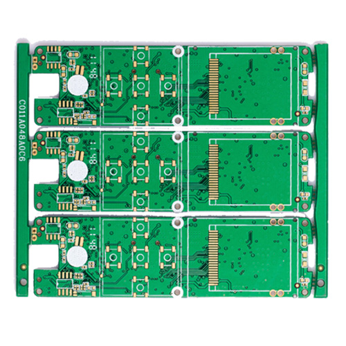
High Capability FR4 Multilayer HDI PCB For Mobile Phone
- HDI PCB
- Mobile Phone
- Multilayer pcb
- fr4 pcb
- Product description: hdi pcb stackup hdi pcb prototype hdi pcb pdf hdi pcb market hdi pcb terminology hdi pcb capability
FR4 Multilayer HDI PCB For Mobile Phone
Quick detail:
|
Material:Fr4 |
|
Layer:4 |
|
Surface finish:immersion gold |
|
Copper weight:1oz |
|
Board size:4.5*3cm |
|
Total thickness:1.6mm |
|
Min line width and space:3mil |
|
Min hole: 0.15mm |
|
Name:High density Interconnector printed circuit boards |
HDI PCB information:
HDI is an abbreviation of High Density Interconnector . It is a kind of circuit board which uses micro blind buried hole technology. HDI is a compact product designed for small-capacity users.
Microvias are used as the interconnects between layers in high density interconnect (HDI) substrates and printed circuit boards (PCBs) to accommodate the high input/output (I/O) density of advanced packages. Driven by portability and wireless communications, the electronics industry strives to produce affordable, light, and reliable products with increased functionality. At the electronic component level, this translates to components with increased I/Os with smaller footprint areas (e.g. flip-chip packages, chip-scale packages, and direct chip attachments), and on the printed circuit board and package substrate level, to the use of high density interconnects (HDIs) (e.g. finer lines and spaces, and smaller vias).
IPC standards define microvias as blind or buried vias with a diameter equal to or less than 150 μm. With the advent of smartphones and hand-held electronic devices, microvias have evolved from single-level to stacked microvias that cross over multiple HDI layers. Sequential build-up (SBU) technology is used to fabricate HDI boards. The HDI layers are usually built up from a traditionally manufactured double-sided core board or multilayer PCB. The HDI layers are built on both sides of the traditional PCB one by one with microvias. The SBU process consists of several steps: layer lamination, via formation, via metallization, and via filling. There are multiple choices of materials and/or technologies for each step.
Microvias can be filled with different materials and processes:filled with epoxy resin (b-stage) during a sequential lamination process step; filled with non-conductive or conductive material other than copper as a separate processing step; plated closed with electroplated copper; screen printed closed with a copper paste. Buried microvias are required to be filled, while blind microvias on the external layers usually do not have any fill requirements.A stacked microvia is usually filled with electroplated copper to make electrical interconnections between multiple HDI layers and provide structural support for the outer level(s) of the microvia or for a component mounted on the outermost copper pad.
HDI PCB application:
Electronic design continues to improve the performance of the whole, while also trying to reduce its size. From mobile phones to smart weapons, small portable products, "small" is always the same pursuit. High-density integration (HDI) technology can make the end product design more compact, while meeting the electronic performance and efficiency of higher standards. HDI is widely used in mobile phones, digital cameras, MP3, MP4, computers, automotive electronics and other digital products, among which the most widely used mobile phones. HDI board generally used to build-up manufacturing, the more the number of layers, the higher the technical grade plate. Ordinary HDI board is basically a laminated, high-level HDI with 2 or more layers of technology, while using stacked holes, electroplating fill, laser drilling and other advanced direct PCB technology. High-end HDI board is mainly used in 3G mobile phones, advanced digital cameras, IC board and so on.
Advantages of HDI PCB:
Can reduce the cost of PCB
Increased Line Density: Interconnecting Traditional Boards to Parts
With better electrical performance and signal correctness
Reliability is better
Can improve the thermal properties
Can improve the radio frequency interference / electromagnetic interference / electrostatic discharge (RFI / EMI / ESD)
Increase design efficiency
Parameter technology of HDI PCB:
|
Feature |
Technical specification |
|
Number of layers |
4 – 22 layers standard, 30 layers advanced |
|
Technology highlights |
Multilayer boards with a higher connection pad density than standard boards, with finer lines/spaces, smaller via holes and capture pads allowing microvias to only penetrate select layers and also be placed in surface pads. |
|
HDI builds |
1+N+1, 2+N+2, 3+N+3,4+N+4, any layer in R&D |
|
Materials |
FR4 standard, FR4 high performance, Halogen free FR4, Rogers |
|
Copper weights (finished) |
18um – 70um |
|
Minimum track and gap |
0.075mm / 0.075mm |
|
PCB thickness |
0.40mm – 3.20mm |
|
Maxmimum dimensions |
610mm x 450mm; dependant upon laser drilling machine |
|
Surface finishes available |
OSP, ENIG, Immersion tin, Immersion silver, Electrolytic gold, Gold fingers |
|
Minimum mechanical drill |
0.15mm |
|
Minimum laser drill |
0.10mm standard, 0.075mm advanced |
Categories
Latest News
Contact Us
Contact: Ms Tracy
Phone: 0086 18682010757
Tel: 0086 18682010757
Add: Building9,Xinyuan Industrial Park,Tangwei,Fuyong,Baoan,Shenzhen,China
 Tracy
Tracy