Multilayer PCB
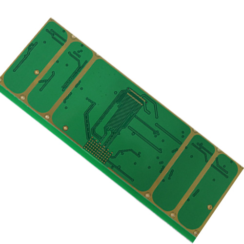
Multilayer Rogers With Fr4 8 Layer Filled Vias PCB Prototype
- filled vias pcb
- via in pad plugging
- copper filled vias pcb
- filled and plated vias
- Product description: filled vias pcb difference between via filling and via plugging kicad filled vias how to fill vias with solder pcb via altium plugged vias pcb planarization via filling with resin via in pad p
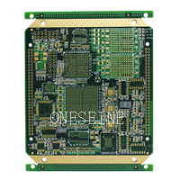
Multilayer Rogers With Fr4 8 Layer Filled Vias PCB Prototype
General information:
Material:Rogers3003 5mi Mix stack up FR4 TG170
Layer:8
Board size: 3.2*5cm
Total thickness: 2.2mm
Copper weight: 0.5OZ
Surface finish: Immersion gold
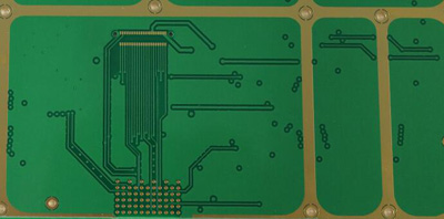
Blind
via Layer 1 to layer 2
Is
an impedance controlled PCB so proof of measured impedance and test coupon to
be supplied
Copper to run to edge
Via filling and over plate ( capped )
Please consult Gerber for full specifications
Filled vias pcb prototype delivery time:6-12 days according to layer number
What’s the difference between resin plug-hole and electroplating hole?
Electroplating hole is vias filled with copper, the hole surface is full of metal,there is no gap, good for welding, but the process requires a high capacity.
Resin plug hole is the hole wall after copper, filled with epoxy resin filled through the hole, and finally the surface of copper, it looks no hole and be good for welding
Via Fill. As a refresher, a via is a copper plated hole that is used to connect two or more layers within a PCB together. Via Fill is a special PCB manufacturing technique used to selectively and completely close via holes with epoxy.
What’s the difference between vias cover oil and green solder mask plug hole
Green solder mask plug hole on the whole process is simple, you can solder in the clean room and surface ink together with the operation. The hole will shrink after curing.For customers who require fullness, this way can not meet the product quality.
Vias cover oil is the hole on the ring ring must be covered with ink, emphasizing the hole edge of the ink coverage. Such as false holes exposed copper, red and so on.
Vias filled PCB:
As a refresher, a via is a copper plated hole that is used to connect two or more layers within a PCB together. Via Fill is a special PCB manufacturing technique used to selectively and completely close via holes with epoxy. There are many instances in which a PCB designer might want to have a via filled. Some key benefits are:
More reliable surface mounts
Increased assembly yields
Improved reliability by decreasing the probability of trapped air or liquids.
Conductive vs. Non-Conductive Via Fill
Non-Conductive Via Fill, sometimes confused with Via Plug, still has copper plated vias to conduct power and heat. The via, however, is filled with a special low shrinkage epoxy specially formulated for this application. Conductive via fill has silver of copper particles distributed throughout the epoxy to provide extra thermal and electrical conductivity.
Non-Conductive fill has a thermal conductivity of 0.25 W/mK whereas Conductive pastes have a thermal conductivity anywhere from 3.5-15 W/mK. In contrast, electroplated copper has a thermal conductivity of more than 250W/mK.
So while Conductive via fill can offer needed conductivity in some applications more often than not it is possible to use non-conductive paste and add additional vias. Often this results in superior thermal and electrical conductivity with minimal cost impact.
Via Filling with Resin
The vias to be filled are filled with a special hole plugging resin, TAIYO THP-100 DX1 thermally curable permanent hole filling material, using a dedicated machine, ITC THP 30. The extra production steps needed for Resin Via Filling are performed before the 2-layer PCB production process. In case of making multi layers, this is after pressing.
Picture2Overview of the extra processes:
Drilling of only the vias that need filling
Cleaning: plasma and brushing
Black Hole
Apply dry resist
Imaging of ONLY the via holes
Via hole galvanization (PTH)
Strip dry resist
Brushing if needed
Baking: 150°C for 1 hour
Via plugging with resin
Baking: 150°C for 1.5 hours
Brushing
Via Filling with Soldermask
The vias to be filled are filled using soldermask ink as hole-filler substance. This Via Filling technology uses a drilled ALU sheet to push normal soldermask ink in the via holes to the filled. This is a screen-printing process. This is a step before the normal soldermask process.
Important:
The filling is always done from the top side of the board
Vias filled with soldermask always get a reverse soldermask pad added with size via-toolsize+0.10mm.
In other words, this Via Filling type will always be covered with soldermask on top and bottom.
Categories
Latest News
Contact Us
Contact: Ms Tracy
Phone: 0086 18682010757
Tel: 0086 18682010757
Add: Building9,Xinyuan Industrial Park,Tangwei,Fuyong,Baoan,Shenzhen,China
 Tracy
Tracy