Printed Circuit Boards
8 Layer PCB Design Fabrication Printed Circuit Boards Production Service
- 4 layer pcb
- 6 layer pcb
- 8 layer pcb
- 10 layer pcb
- Product description: pcb design software pcb assembly pcb fabrication process pcb manufacturer for hobbyist online pcb design and manufacture how to make a custom pcb PCB design online PCB design tutorial PCB desi
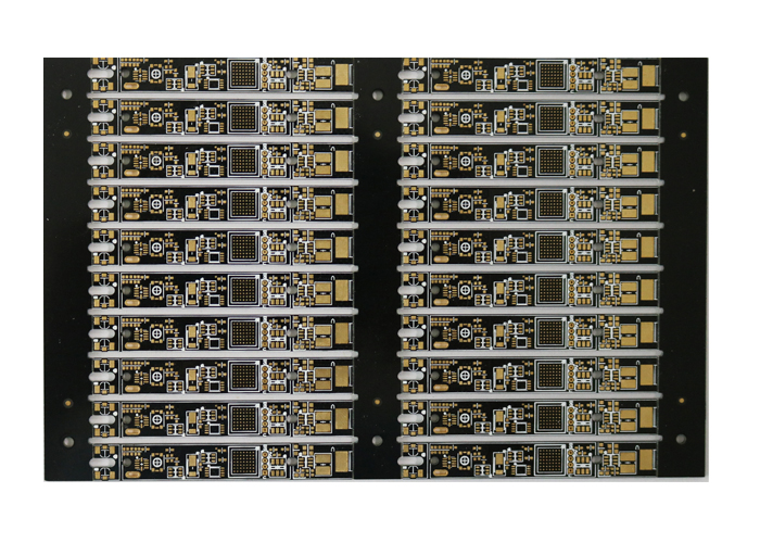
8 Layer PCB Design Fabrication printed circuit boards Production Service
Basic information:
Board size: 16*15CM
Layer: 8 layer printed circuit board
Solder mask: Black
Copper weight: 2OZ
Material: FR4
Name: 8 layer Multilayer PCB fabrication
Blind hole and via filled and capped:yes
Min line:4mil
Min hole:0.25MM
The difference of 4/6/8 layer pcb:
Generally 4 layer pcb: SIG→GND(PWR)→PWR(GND)→SIG
6 layer pcb have 3 different arrange way
8 layer pcb have 3 different arrange way,see below:
First
1 Signal 1 components side, microstrip line layer
2 Signal 2 inner microstrip line layer
3 Ground
4 Signal 3 Stripline line layer
5 Signal 4 Stripline line layer
6 Power
7 Signal 5 inner microstrip line layer
8 Signal 6 microstrip line layer
Second
Due to the increase of the reference layer, with good EMI performance, the signal layer of the characteristic impedance can be well controlled
1 Signal components side, microstrip line layer
2 Ground GND,Good electromagnetic wave absorption capacity
3 Signal Stripline line layer
4 Power PWR, and the underlying formation constitutes excellent electromagnetic absorption
5 Ground GND
6 Signal Stripline line layer
7 Power GND, With a large power supply impedanc
8 Signal Stripline line layer
Third:
The best stacking mode, because the use of multilayer ground reference plane has a very good magnetic absorption capacity
1 Signal components side, microstrip line layer
2 Ground GND,Good electromagnetic wave absorption capacity
3 Signal Stripline line layer
4 Power PWR, and the underlying formation constitutes excellent electromagnetic absorption
5 Ground GND
6 Signal Stripline line layer
7 Ground GND,Good electromagnetic wave absorption capacity
8 Signal Stripline line layer
EMC of these types of circuit boards is still a big difference, if it is high-speed version, then consider EMC, then at least 8 layers, 4 signal layers, in accordance with the signal - ground - signal - ground - power - signal - ground Of the arrangement in order to take the four signal layers are high-speed signal lines
How to design multilayer pcb layer number:
For how to choose the design with multilayers and the stack, need according to the number of signal on the circuit board, device density, PIN density, signal frequency, board size and many other factors. For these factors we have to consider. The more the number of signal networks, the greater the density of the device, the greater the density of the PIN, the higher the frequency of the signal should be designed with multilayer design. It is best to ensure that each signal layer has its own reference layer for good EMI performance.
Categories
Latest News
Contact Us
Contact: Ms Tracy
Phone: 0086 18682010757
Tel: 0086 18682010757
Add: Building9,Xinyuan Industrial Park,Tangwei,Fuyong,Baoan,Shenzhen,China
 Tracy
Tracy